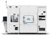
Features
The only wafer fab AFM with automatic defect review
Fully automated AFM solution for defect imaging and analysis that improves defect review productivity by up to 1,000%
Park's Smart ADR provides fully automated defect review and identification, enabling a critical inline process to classify defect types and source their origin through high resolution 3D imaging.
Designed specifically for the semiconductor industry, Smart ADR is the most advanced defect review solution available, featuring automatic target positioning without the need for labor intensive reference marks that often damage the sample. The Smart ADR process improves productivity by up to 1,000% compared to traditional defect review methods. Additionally, the new ADR capability offers up to 20x longer tip life thanks to Park's groundbreaking True Non-Contact™ Mode AFM technology.
Low noise Atomic Force Profiler for accurate, high throughput CMP profile measurements
The industry leading low noise Park AFM is combined with a long range sliding stage to become an Atomic Force Profiler (AFP) for chemical mechanical polishing (CMP) metrology. The new low noise AFP provides very flat profiling for both local and global uniformity measurements with the best profiling accuracy and repeatability on the market. Unique True Non-Contact™ mode enables nondestructive in-line measurements with much longer tip life, while Park's innovative True Sample Topography™ obtains CMP profiles without the usual artifacts associated with a traditional piezotube-based AFP. This guarantees accurate height measurements with no non-linear or high noise background subtraction over a wide range of profiling lengths.
Sub-Angstrom surface roughness measured with extreme accuracy and minimized tip-to-tip variation
The surface roughness of a wafer is critical in determining the performance of a semiconductor device. For the state-of-the-art device manufacturer, both chip makers and wafer suppliers are demanding more accurate roughness control of ultra-flat surface on Si or SOI wafers. By delivering the industry’s lowest noise floor of less than 0.5 Å and combining it with True Non-Contact™ mode, Park NX-Wafer can reliably acquire sub-Angstrom roughness measurements with minimum tip-to-tip variation. Park's Crosstalk Elimination also allows very flat orthogonal XY scanning with no background curvature, even on the flattest of surfaces regardless of scan location, rate, and size. This enables very accurate and repeatable surface measurement from micro-roughness to long-range waviness.
Specifications
System Specification
Motorized XY stage
200mm : travels up to 275 mm × 200 mm, 0.5 µm resolution
300mm : travels up to 400 mm × 300 mm, 0.5 µm resolution, 1 µm repeatability
Motorized Z stage
25 mm Z travel distance,
0.08 µm resolution, < 1 µm repeatability
Motorized Focus Stage
9 mm Z travel distance for on-axis optics
Sample Thickness Allowance
up to 20 mm
Full scan range Z run-out
< 2 nm, repeatability < 1nm
COGNEX Pattern Recognition
pattern align resolution of 1/4 pixel

 SingaporeSG
 ChinaCN
 MalaysiaMY
 IndonesiaID
 MyanmarMM


